
NCS 5500 Buffering Architecture
The NCS 5500 uses an innovative design to provide deep buffering while maintaining high performance and power efficiency. This paper explores this design and shows its strengths over traditional forwarding architectures. It also will address criticism of these optimizations coming from other vendors.
Executive Summary
Buffers are the shock absorbers in networks. Their primary role is to manage temporary congestion in a manner that controls loss and latency while allowing end nodes to adapt to available bandwidth or complete short transfers without loss. Note that this does not mean preventing all packet loss and that buffers cannot solve persistent or artificial congestion that does not respond to signals from the network.
Router Buffering Architectures
Off-chip vs. On-chip buffering
One of the tradeoffs a router architect needs to make is where to buffer packets. Traditionally, there have been two options: on-chip or off-chip.
On-chip buffering minimizes power and board space but doesn’t allow for buffering beyond 10s or 100s of microseconds. It is well suited to data centers where round trip times allow end nodes to adjust their speed very quickly and where bandwidth can be overprovisioned via inexpensive fiber runs. In some cases, it may still have limitations due to TCP Incast traffic flows. On-chip SRAM buffers are a 10,000th the size of off-chip buffers so it’s not a small difference. On-chip buffering allows for higher-bandwidth devices as it allows more of the ASIC’s resources to be used for physical ports rather than connecting to off-chip memories. On-chip vs. off-chip buffering is one of the key factors underlying the wide range of port counts and power consumption between routers with the two models. As of 2018, fabric-capable forwarding chips with off-chip buffers currently range from 200 to 900 Gbps while System on Chip models shipping range up to 3.2 Tbps.
With off-chip buffering, two key requirements must be met. First, the memory must be large enough to buffer the required packets. This is a separate topic, but note that the NCS 5500 ha very large buffers. Second, it must be fast enough to maintain the forwarding rate. The bandwidth component of memory performance is a key challenge for buffering. This paper discusses how the NCS 5500 balances the bandwidth constraint with other design goals such as performance, power, and cost.
For deep buffers, a router architect must currently choose between high-speed custom memories or large banks of commodity memories. While not as difficult as FIB memory requirements (which require high operations per second), memory bandwidth can be a challenge as commodity memories are not designed for the operations needed for networking. Traditionally, deep-buffered routers pass every packet through the off-chip memory. Note that these memories are also used for forwarding tables, which may or may not be stored in the same memory bank.
High-performance memories can be made to a wide range of specifications, including bandwidth, operations per second, capacity, cost, and physical size. They save board space but are significantly more expensive and consume more power as performance increases.
Off-chip buffering with commodity memory is less expensive but often requires more board space than custom memories due to the need to overprovision the capacity in order to get sufficient aggregate memory bandwidth.
Using a mid-performance commodity memory such as graphics memory (e.g., GDDR5) helps, but still doesn’t meet the performance of high-end memory devices.
Cisco uses custom high-performance memories on the CRS and NCS 6000. Commodity memory is used for buffering on the ASR 9000 and NCS 5500. The NCS 5000 has on-chip buffers only.
Motivation for a New Design
There are two key drivers for rethinking the traditional approach to off-chip buffers when designing new chips. First, valuable bandwidth (and thus power) is used to perform an off-chip write/read for packets that don’t require moderate or deep buffers. Second, in the near future even high-performance memories will no longer be able to keep up with the requirements of ASICs as silicon logic and on-chip memory will continue to outpace off-chip memory performance.
An Innovative Approach – Hybrid Buffering
New chip designs must address the memory bandwidth challenge while still acheiving the overall system goals to balance price, performance, power, and functionality. Commodity memory bandwidth currently maxes out at approximately 900G half duplex. High-performance memories are available supporting 400G & 500G ASICs at line rate (some are ~500G full duplex, others are ~1T half duplex). Future generations of custom memory (notably HBM which is discussed later) will increase performance but still not be able to keep up with highest-bandwidth processors.
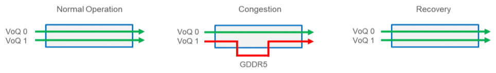
A solution to this challenge to implement both on-chip and off-chip buffers and only use off-chip buffers as needed. This is the design of the NCS 5500. Packets in congested queues are buffered off-chip while packets in empty and lightly congested queues (less than approximately 5000 packets) remain on-chip. This is called an evict / readmit model in which queues can transition on and off chip as they fill or empty. It uses memory bandwidth more efficiently and allows the chip to run faster than the off-chip memory. This approach has an additional benefit of reduced power consumption relative to buffering all packets off-chip.
This design is based on the same principle that underlies much of network and server design – statistical multiplexing. Not all clients (of the network or of memory) need to use the full bandwidth at the same time. This oversubscription is small for the worst-case and negligible in practice in Jericho and Jericho+. Oversubscription will increase in the future as the gap between memory technologies and forwarding logic continues to grow so this design will become even more critical in the future.
The next section explains how hybrid buffering is implemented in NCS 5500. Later, the conditions needed to see corner cases in the lab are explained.
Jericho ASIC Architecture
The diagram below shows a high-level view of the Jericho & Jericho+ ASICs used in NCS 5500. There are two packet cores. The cores share on-chip buffers with separate pools for ingress and egress (OTM in the graphic). The on-chip buffers are approximately 16MB each. The egress buffer supports reassembling packets but doesn’t provide externally visible QoS. In addition, it doesn’t drop packets due to the VoQ scheduling, which only allows packets to be sent to egress once they can be transmitted. The configured QoS is implemented by the ingress traffic manager. The ingress on-chip buffer contains VoQs for every output queue in the system. A vast majority of packets pass only through these on-chip buffers.
If a queue becomes moderately congested, the queue is “evicted” and additional packets for that queue only will be stored in an off-chip GDDR5 memory. Eviction occurs on a per-queue basis so all other traffic to the destination physical port and all other ports remains in the on-chip buffers.
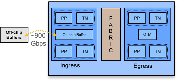 Figure 1: Jericho ASIC Logical Diagram
The aggregate half-duplex bandwidth between the forwarding cores and the off-chip memory is approximately 900 Gbps. With GDDR5, this bandwidth can be used for read or write, which is an important component of the design as, in theory, even line rate bursts on all interfaces on 900G Jericho+ can be absorbed before shifting the bandwidth allocation back to read the packets out. In Jericho, at very high levels of memory bandwidth usage, writes are given a higher priority in order to absorb large bursts into deep queues. With sustained high rates near the maximum memory bandwidth, the allocation will return to 50/50 to allow the off-chip buffers to drain. At that point, packet loss is inevitable in any router so managing the drops becomes very important. If the allocated write bandwidth is exceeded, packets for the specific queues that are tail dropping in the off-chip memory will temporarily be dropped on-chip. This preserves memory bandwidth for packets that may not need to be dropped. Packets to other queues utilizing the deep buffers will receive priority for storage in off-chip memory. Meanwhile, the configured QoS policies are being implemented, which may further reduce the memory bandwidth required.
Some other memory technologies do not have the flexibility of half duplex bandwidth that can be shared between read and write. In practice, that is not an issue today, but may be a challenge in the future.
This condition is clearly an extreme and contrived corner case. It will only be seen in a lab test with a traffic generator and almost every packet forced to heavily congested queues.
Deep Buffering
The NCS 5500 can provide extremely deep buffers when required. This is enabled by the size of the off-chip memory as well as the distributed VoQ architecture. The off-chip memory on each chip is 4 GB and can store up to 3 million packets (1.5M packet descriptors on each core). After buffer carving, the effective capacity is approximately 3GB.
There are also system-level factors that are key to the buffering architecture in multi-ASIC systems (the 2 RU NCS 5502, the line card based NCS 5504/5508/5516, and the newer 1 RU systems with multiple Jericho+ ASICs). When significant congestion of a VoQ is occurring, it is likely to enter the router on more than one NPU. This means that the aggregate memory available for buffering to a single egress queue comprises the memory on all ingress ASICs receiving traffic destined to that queue. When this is occurring, each ASIC individually moves queues on and off-chip as needed. With this model, the total buffering for a queue is larger than any router with two-stage queuing.
When all the ingress traffic enters a single ASIC (such as the single-chip NCS 5501) the system can buffer up to approximately 30 msec on all ports at the same time when all traffic is going to congested output queues. If fewer queues are congested, more memory is available to the congested queues, up to 1 GB and 390k packets per queue.
The default queue depths on NCS 5500 are set to 10 msec per NPU, but they can be increased significantly if required by the network designer. Care should be taken as too much buffering can cause just as many problems as not enough.
For a practical analysis of memory capacity and bandwidth, it is important to understand that all the queues will not be highly congested at the same time.
Future ASIC Architecture Direction
Increases in ASIC logic and on-chip memory performance will continue to outpace off-chip memory. This gap will grow significantly over time. In the near future, many routers with high-end custom memories will need to embrace this model. The only other option is to use an increasing number of relatively small ASICs, still with high- performance memories.
In 2018 or 2019, networking ASICs will begin shipping with a new technology called High Bandwidth Memory (HBM). HBM is a high-end commodity component that must be tightly integrated with the on-die logic by placing it into the ASIC package. This new option will deliver a significant increase in memory bandwidth as well as a decrease in power.
Summary
This paper has shown the benefits of the hybrid buffering architecture and how it is implemented on Cisco’s NCS 5500 routers. It has also addressed the criticism of this design. While it should be clear that hybrid buffering is an optimal design in many cases, Cisco will still be implementing the traditional off-chip approach, especially in extensions to existing platforms.
Leave a Comment